

Near-Field & Cable Probes for EMC troubleshooting
Near-field probes for EMC testing are commercially available, but fairly expensive. Yet, they are easy to make, using no more than rigid (or semi-rigid) coax cable and a SMA connector. “Do-It-Yourself” near-field probes have been covered at various sites. For example, in EEVblog #1178 David Jones showed how create a H-field probe for $10 that performs equivalently to a commercial $300 one. My contribution is not so much an improvement to the “electrical” aspect of the probes, but an adjustable design for an insulated sleeve for the probe.
-
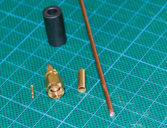
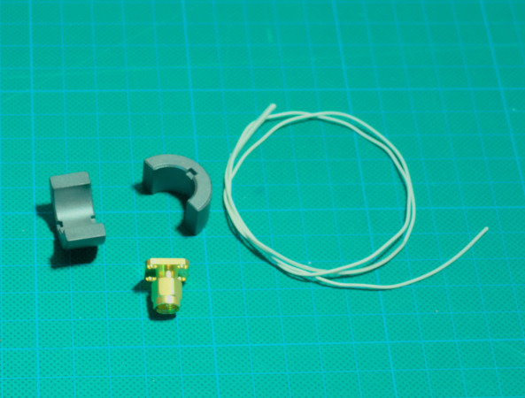
materials
-
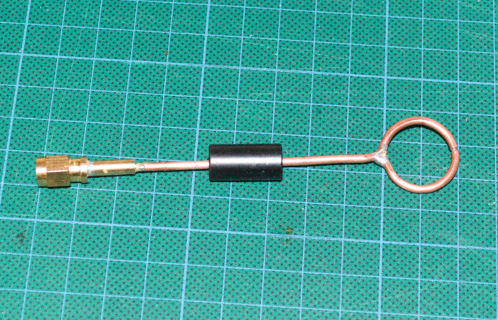
basic probe
-

printed sleeve
-
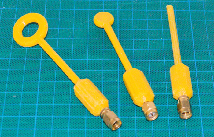
completed
probes
Near-field probes must be made from 50Ω coax cable. Nearly all designs I found on the web use semi-rigid coax cable, because it is easier to bend. I prefer (unjacketed) 2.5mm rigid cable myself: it is thin enough to be bendable (with tools) and cutting a neat narrow groove in the shield (outer conductor) is easier to do in solid copper than in braided wire.
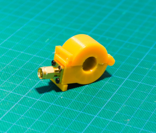
Since you put near-field probes very near or on components, pads and traces, the probes should be insulated. Otherwise, you risk shorting pins when the probe touches two pads at the same time. My solution is to put the probes inside a 3d-printed plastic sleeve.
If you are creating your own probes, each will probably be unique in its dimensions: the loop diameter, the length of the wand, the size of the ferrite bead (and whether there is a ferrite bead at all)… Which is why publishing a set of STL files won't be of any use: your near-field probes will almost certainly have different dimensions than mine. And therefore, the download below is for the OpenSCAD design file. The important parameters can all be adjusted with the “Customizer” of OpenSCAD. The insulating sleeves pictured on this page were all created from the same design file, after adjusting the options.
Basic design of a H-field probe
An H-field probe is a ring. Where the ring closes on the wand, there is a solder joint to connect the shield of the coax from end of the ring to its beginning. Furthermore, at this point, the centre wire of the coax is soldered to the shield. In the schematic figure below, these solder joints are indicated by a red dot (in reality, the solder of the shield goes all around). And finally, at the opposite site of the ring, the shield is interrupted by a narrow groove (the centre wire is continuous).
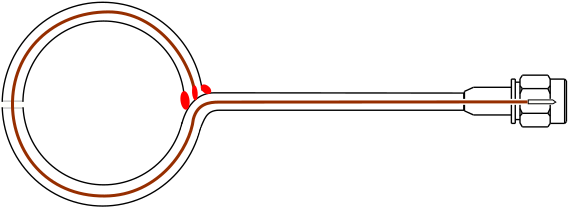
The only thing left to do is to solder an SMA connector to the other end of the wand. A ferrite bead near the SMA connector is recommended, to reduce noise on the “ground” line, but the probe also works without it.
Design of an HF current clamp
Although you can use an H-field probe to check for common-mode currents on a cable, an HF current clamp is more sensitive and more practical.
The basic design of a current clamp is a ferrite ring and a wire that winds around it. The number of windings is not critical; it is usually between 10 and 16 for a full ring. The windings are evenly spaced, so that the capacitance between them is minimal. In practice, however, a design with two half-rings is more common, because these are easily snapped around the cable. The wire is only wound around one half (and therefore there are commonly between 5 and 8 windings).
My design is based on the Würth snap-on ferrite number 7427141. The plastic case that this ferrite has is discarded: we will need a new case with a bit more space to allow for the windings, a hinge that allows for frequent opening and closing, and a SMA connector. Incidentally, the connector I have used is Amphenol RF 132166.
-
materials
-

partial
assembly -
completed clamp
The Downloads section includes a STL file for the sleeve of the HF current clamp (unlike the sleeve for the near-field probes). If you use the same ferrite core and the same SMA connector (and wire for the windings with a diameter close to 0.9mm), it should all fit in the readily printable STL file. Otherwise, use the OpenSCAD design file and adjust the parameters.
Kenneth Wyatt recommends that conductive tape be wrapped over the windings, as a shield against the E-field (see the References). However, a test by Olli Väänänen of two identical HF current probes except that one was shielded and the other was not, showed no relevant differences. The effect of shielding is therefore insignificant in practice.
A word on the quality & calibration …
Manufacturers and professional users sometimes claim that commercial probes merit their price because of the intricate design needed to make them suitable for a wide frequency range. This refers to the design of most commercial probes: they are actually made as a four-layer PCB, where the outer layers form the shield and one of the inner layers has the centre conductor. Along the edges are plenty of vias to connect the top and bottom layers and create, sort-of, a full shield. The difficulty, now, is to control the impedance over the entire stripline.
Companies choose this design, because it is easy to machine-produce. But if a bit of tinkering and hand-soldering are not an issue, there is an immediate advantage of using (semi-)rigid coax: you can readily get it with the correct impedance and optimized for a wide frequency range. These do-it-yourself probes can easily achieve the same professional-grade quality as the commercial probes.
The criterion of whether a device passes or fails EMC compliance, is based on the measurements in the far field. For near field probes, there is, however, no way to extrapolate the measurements into equivalent far-field results. This is why I do not see any merit in purchasing calibrated near-field probes. The quantitative result of a near-field measurement simply isn't useful. (See also the References below.)
For an HF current clamp, the situation is different: if an HF current clamp is calibrated (the more accurate term is “characterized”), the amount of far-field emission that is radiated from the cable can be calculated from the measurements of the current clamp. And so, a calibrated HF current clamp allows you to make far-field predictions from simple measurements that you do with relatively inexpensive equipment in your office. If you wish to characterize your home-built HF current probe, check Olli Väänänen's paper and the March 2012 article by Kenneth Wyatt in the References.
That said, the far-field prediction is only valid for the radiated emission from a single cable. Emission from multiple cables cannot simply be added together, but these do contribute to the overall emission. Radiated emission directly from the device (as opposed to that from cables attached to the device) is not accounted for at all. As a result, the only conclusion that a calibrated HF current clamp will allow you to draw is that a product will definitely fail compliance if the measurements on any single cable exceed a limit. In our experience, this is an unlikely scenario (and even with an uncalibrated HF current clamp, the peaks will stand out). It is why we decided that calibration (or “characterization”) of an HF current clamp is not worth the effort.
… And a word testing strategy
As stated above, near-field measurements do not translate to far-field predictions. We will have to make do with a (qualitative) rule of thumb:
- When a peak frequency shows up in the far-field test, it is guaranteed to also pop up in near-field probing.
- The inverse is not true, however: a peak that is prominent in the near-field test may not be significant (or even discernible) in the far-field test.
The oft-repeated advice, therefore, is to do a far-field (pre-)compliance test first and to troubleshoot only the critical peaks that showed up in that test. The idea is to avoid spending time on “fixing” non-existent problems.
As valid as this advice may be, it overlooks another truism: when no significant peak surfaces in the near-field test, none can pop up in the far-field test either. The point is, (pre-)compliance testing is expensive. It is also done at the end of the design cycle. Since adjustments late in the design cycle are usually quite more expensive than if they had been done early on, there is also the tendency to look for a quick fix: a “shielding can” over the culprit, conductive spray on the inside of the plastic enclosure, ferrite beads on the cables that you provide with the product (because it's too late to put the ferrites inside the product), and so on…
When potential EMC problems are tackled early on, however, in many cases the required modifications are cheap, for example:
- adding a series resistor on a high-frequency output (or oscillator) to reduce the slew rate of the signal;
- adding a ferrite bead on the power rail (because the traces of the power rail run over all of the board);
- routing a critical trace differently (or the traces around the critical trace), for example to achieve a more tightly coupled ground-return path;
- etcetera…
In the early stages, the design is still in flux and it is likely that other adjustments also need to be made. The modifications that address the (potential) EMC problems can then simply be slipped in, without adding much extra time or costs. Of course, not every near-field emission will have a cheap fix, but yet my recommendation is:
- verify the near-field performance throughout the design process, starting with the first prototype;
- identify the culprit of each notable peak, and consider what measures need to be taken to mitigate the potential problem;
- if there is a simple and cheap fix → implement it; if there isn't → make a note of the peak and what causes it, but postpone the decision whether or not to fix it until after the (pre-)compliance test.
Downloads
| Design file for the near-field probe sleeves | OpenSCAD |  |
| Design file for the HF current clamp sleeve | OpenSCAD | |
| STL file for the HF current clamp sleeve (see text) | STL | |
Links
| OpenSCAD | www.openscad.org |
References
| Workbench EMC Measurements | Henry W. Ott, 2013 |
| Do-It-Yourself current probe characterization for EMC troubleshooting | Olli Väänänen; 2014 International Symposium on Fundamentals of Electrical Engineering |
| Assembling A Low Cost EMI Troubleshooting Kit - Part 1 | Kenneth Wyatt; Interference Technology; May 2016 |
| The HF Current Probe: Theory and Application | Kenneth Wyatt; Interference Technology; March 2012 |
